- 您现在的位置:买卖IC网 > Sheet目录471 > MAX2009ETI+T (Maxim Integrated)IC RF PREDISTORT ADJ 28-TQFN
�� �
�
�1200MHz� to� 2500MHz� Adjustable�
�RF� Predistorter�
�ABSOLUTE� MAXIMUM� RATINGS�
�V� CCG� ,� V� CCP� to� GND� ..............................................-0.3V� to� +5.5V�
�ING,� OUTG,� GCS,� GFS,� GBP� to� GND......-0.3V� to� (V� CCG� +� 0.3V)�
�INP,� OUTP,� PFS_,� PDCS_,� PBRAW,�
�PBEXP,� PBIN� to� GND� ............................-0.3V� to� (V� CCP� +� 0.3V)�
�Input� (ING,� INP,� OUTP,� OUTG)� Level� ............................+23dBm�
�PBEXP� Output� Current� ........................................................� ±� 1mA�
�Continuous� Power� Dissipation� (T� A� =� +70� °� C)�
�28-Pin� Thin� QFN-EP�
�(derate� 21mW/� °� C� above� +70� °� C)� ...............................1667mW�
�Operating� Temperature� Range� ...........................-40� °� C� to� +85� °� C�
�Junction� Temperature� ......................................................+150� °� C�
�Storage� Temperature� Range� .............................-65� °� C� to� +150� °� C�
�Lead� Temperature� (soldering� 10s)� ..................................+300� °� C�
�Stresses� beyond� those� listed� under� “Absolute� Maximum� Ratings”� may� cause� permanent� damage� to� the� device.� These� are� stress� ratings� only,� and� functional�
�operation� of� the� device� at� these� or� any� other� conditions� beyond� those� indicated� in� the� operational� sections� of� the� specifications� is� not� implied.� Exposure� to�
�absolute� maximum� rating� conditions� for� extended� periods� may� affect� device� reliability.�
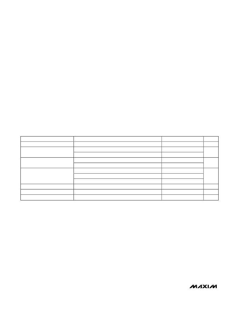
�DC� ELECTRICAL� CHARACTERISTICS�
�(MAX2009� EV� kit;� V� CCG� =� V� CCP� =� +4.75V� to� +5.25V;� no� RF� signal� applied;� INP,� ING,� OUTP,� OUTG� are� AC-coupled� and� terminated� to�
�50� Ω� ;� V� PF_S1� =� open;� PBEXP� shorted� to� PBRAW;� V� PDCS1� =� V� PDCS2� =� 0.8V;� V� PBIN� =� V� GBP� =� V� GCS� =� GND;� V� GFS� =� V� CCG� ;� T� A� =� -40� °� C� to�
�+85� °� C.� Typical� values� are� at� V� CCG� =� V� CCP� =� +5.0V,� T� A� =� +25� °� C,� unless� otherwise� noted.)�
�PARAMETER�
�CONDITIONS�
�MIN�
�TYP�
�MAX�
�UNITS�
�Supply� Voltage�
�Supply� Current�
�Analog� Input� Voltage� Range�
�Analog� Input� Current�
�V� CCG� ,� V� CCP�
�V� CCP�
�V� CCG�
�PBIN,� PBRAW�
�GBP,� GFS,� GCS�
�V� GFS� =� V� GCS� =� V� PBRAW� =� 0V�
�V� GBP� =� 0� to� +5V�
�V� PBIN� =� 0� to� +5V�
�4.75�
�0�
�0�
�-2�
�-100�
�-100�
�5.8�
�10�
�5.25�
�7�
�12.1�
�V� CCP�
�V� CCG�
�+2�
�+170�
�+220�
�V�
�mA�
�V�
�μA�
�Logic-Input� High� Voltage�
�Logic-Input� Low� Voltage�
�PDCS1,� PDCS2� (Note� 1)�
�PDCS1,� PDCS2� (Note� 1)�
�2.0�
�0.8�
�V�
�V�
�Logic� Input� Current�
�-2�
�+2�
�μA�
�2�
�_______________________________________________________________________________________�
�发布紧急采购,3分钟左右您将得到回复。
相关PDF资料
MAX2010ETI+T
IC RF PREDISTORT ADJ 28-TQFN
MAX2014ETA+T
IC DETECT/CNTRL LOG 8-TDFN
MAX2015EUA+T
IC DETECT/CNTRL LOG 8-UMAX
MAX2015EVKIT
EVAL KIT FOR MAX2015
MAX2016ETI+T
IC DETECT/CNTRL LOG 28-TQFN
MAX2021ETX+T
IC MOD/DEMOD 36-TQFN
MAX2022ETX+T
IC MOD 1500MHZ TO 2500MHZ 36TQFN
MAX2022EVKIT
EVAL KIT FOR MAX2022
相关代理商/技术参数
MAX2009ETI-T
功能描述:射频前端 1.2-2.5GHz Adj RF Predistorter RoHS:否 制造商:Skyworks Solutions, Inc. 类型: 工作频率:2.4 GHz, 5 GHz 最大数据速率:54 Mbps 噪声系数: 工作电源电压:3.3 V 电源电流:180 mA 最大工作温度:+ 85 C 安装风格:SMD/SMT 封装 / 箱体:QFN-32
MAX2009EVKIT
功能描述:射频开发工具 Evaluation Kit for the MAX2009 MAX2010 RoHS:否 制造商:Taiyo Yuden 产品:Wireless Modules 类型:Wireless Audio 工具用于评估:WYSAAVDX7 频率: 工作电源电压:3.4 V to 5.5 V
MAX200C/D
功能描述:RS-232接口集成电路 +5V RS-232 Transceiver with 0.1 Micro Farads External Capacitors RoHS:否 制造商:Exar 数据速率:52 Mbps 工作电源电压:5 V 电源电流:300 mA 工作温度范围:- 40 C to + 85 C 安装风格:SMD/SMT 封装 / 箱体:LQFP-100 封装:
MAX200CPP
功能描述:RS-232接口集成电路 RoHS:否 制造商:Exar 数据速率:52 Mbps 工作电源电压:5 V 电源电流:300 mA 工作温度范围:- 40 C to + 85 C 安装风格:SMD/SMT 封装 / 箱体:LQFP-100 封装:
MAX200CWP
功能描述:RS-232接口集成电路 RoHS:否 制造商:Exar 数据速率:52 Mbps 工作电源电压:5 V 电源电流:300 mA 工作温度范围:- 40 C to + 85 C 安装风格:SMD/SMT 封装 / 箱体:LQFP-100 封装:
MAX200CWP+
功能描述:RS-232接口集成电路 5V RS-232 Tcvr w/0.1uF External Cap RoHS:否 制造商:Exar 数据速率:52 Mbps 工作电源电压:5 V 电源电流:300 mA 工作温度范围:- 40 C to + 85 C 安装风格:SMD/SMT 封装 / 箱体:LQFP-100 封装:
MAX200CWP+T
功能描述:RS-232接口集成电路 5V RS-232 Tcvr w/0.1uF External Cap RoHS:否 制造商:Exar 数据速率:52 Mbps 工作电源电压:5 V 电源电流:300 mA 工作温度范围:- 40 C to + 85 C 安装风格:SMD/SMT 封装 / 箱体:LQFP-100 封装: